NEWS AGILEX FPGAS
SureCore unveils low
power design service
SureCore, the low power SRAM IP specialist,
has opened a new Low Power Design Service
that offers its concept-to-tape-out low power
mixed-signal design expertise to ASIC
developers.
Its Design Service targets the pervasive
system-centric low power design challenge
through a comprehensive suite of low-power
mixed signal services, including design and
layout capabilities, technology porting, as well
as low voltage veri cation and characterization.
These services span bulk nodes from 55nm to
leading-edge advanced nodes.
“One of the trends driving the re-birth of
ASICs is that off-the-shelf devices do not
deliver system-level differentiated functionality.
We’re seeing this to be particularly true for
low-power ASIC design, particularly those that
involve mixed-signal functionality,” said Paul
Wells, sureCore CEO.
“We’ve solved these challenges in the
past and are now offering the same design
capability that delivered market-leading,
custom, low power SRAM solutions in
advanced FinFET processes. Many of these
successes targeted demanding networking and
imaging application,” he explained.
SureCore’s design capabilities cover
a wide range of the most commonly used
circuit blocks including ADCs, DACs,
Ampli ers, Regulators, LDOs, Phase-Lock
Loops, Oscillators, Bandgaps, Comparators,
Programmable Current Mirrors, POR and
Brown-Out.
Porting and custom layout services are
offered across many foundries and process
nodes with silicon-proven experience including
Bulk, FDSOI and FinFET nodes.
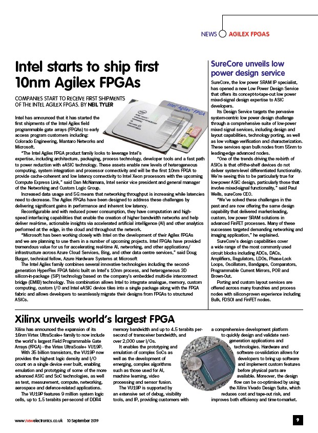
Intel starts to ship fi rst
10nm Agilex FPGAs
COMPANIES START TO RECEIVE FIRST SHIPMENTS
OF THE INTEL AGILEX FPGAS. BY NEIL TYLER
Intel has announced that it has started the
rst shipments of the Intel Agilex eld
programmable gate arrays (FPGAs) to early
access program customers including:
Colorado Engineering, Mantaro Networks and
Microsoft.
“The Intel Agilex FPGA product family looks to leverage Intel’s
expertise, including architecture, packaging, process technology, developer tools and a fast path
to power reduction with eASIC technology. These assets enable new levels of heterogeneous
computing, system integration and processor connectivity and will be the rst 10nm FPGA to
provide cache-coherent and low latency connectivity to Intel Xeon processors with the upcoming
Compute Express Link,” said Dan McNamara, Intel senior vice president and general manager
of the Networking and Custom Logic Group.
Increased data usage and 5G means that networking throughput is increasing while latencies
need to decrease. The Agilex FPGAs have been designed to address these challenges by
delivering signi cant gains in performance and inherent low latency.
Recon gurable and with reduced power consumption, they have computation and highspeed
interfacing capabilities that enable the creation of higher bandwidth networks and help
deliver real-time, actionable insights via accelerated arti cial intelligence (AI) and other analytics
performed at the edge, in the cloud and throughout the network.
“Microsoft has been working closely with Intel on the development of their Agilex FPGAs
and we are planning to use them in a number of upcoming projects. Intel FPGAs have provided
tremendous value for us for accelerating real-time AI, networking, and other applications/
infrastructure across Azure Cloud Services, Bing, and other data centre services,” said Doug
Burger, technical fellow, Azure Hardware Systems at Microsoft
The Intel Agilex family combines several innovative technologies including the secondgeneration
HyperFlex FPGA fabric built on Intel’s 10nm process, and heterogeneous 3D
silicon-in-package (SiP) technology based on the company’s embedded multi-die interconnect
bridge (EMIB) technology. This combination allows Intel to integrate analogue, memory, custom
computing, custom I/O and Intel eASIC device tiles into a single package along with the FPGA
fabric and allows developers to seamlessly migrate their designs from FPGAs to structured
ASICs.
Xilinx unveils world’s largest FPGA
Xilinx has announced the expansion of its
16nm Virtex UltraScale+ family to now include
the world’s largest Field Programmable Gate
Arrays (FPGA) - the Virtex UltraScale+ VU19P.
With 35 billion transistors, the VU19P now
provides the highest logic density and I/O
count on a single device ever built, enabling
emulation and prototyping of some of the more
advanced ASIC and SoC technologies, as well
as test, measurement, compute, networking,
aerospace and defence-related applications.
The VU19P features 9 million system logic
cells, up to 1.5 terabits per-second of DDR4
memory bandwidth and up to 4.5 terabits persecond
of transceiver bandwidth, and
over 2,000 user I/Os.
It enables the prototyping and
emulation of complex SoCs as
well as the development of
emerging, complex algorithms
such as those used for AI,
machine learning, video
processing and sensor fusion.
The VU19P is supported by
an extensive set of debug, visibility
tools, and IP, providing customers with
a comprehensive development platform
to quickly design and validate nextgeneration
applications and
technologies. Hardware and
software co-validation allows for
developers to bring up software
and implement custom features
before physical parts are
available. Moreover, the design
ow can be co-optimised by using
the Xilinx Vivado Design Suite, which
reduces cost and tape-out risk, and
improves both ef ciency and time-to-market.
www.newelectronics.co.uk 10 September 2019 9
/www.newelectronics.co.uk