ANALOGUE DESIGN ANTENNAS
Monolithic GaN ICs are capable of
delivering over 100 W of power with
over 50% PAE. Combining this level
of efficiency with the low duty cycle of
radar applications allows for surfacemount
solutions where it is possible
to dissipate the heat generated
through the package base.
High reliability designs may
use gold plated, hermetically
sealed housing with chip-and-wire
interconnects inside and are more
robust for extreme environments, but
are larger and more costly.
Multichip modules (MCMs)
combine numerous MMIC devices,
as well as passives, into a relatively
low cost surface-mount package.
MCMs still allow for the mixing of
semiconductor technologies so that
the performance of each device
can be maximized while saving
considerable space.
Phased array beamformer ICs
Integrated analogue beamforming
ICs - core chips - are being
developed to support a range of
applications. The primary function
of these chips is to accurately
set the relative gain and phase of
each channel so that signals add
coherently in the desired direction of
the antenna main beam.
They are being developed for
analogue phased array applications
or hybrid array architectures that
combine some digital beamforming
with analogue beamforming.
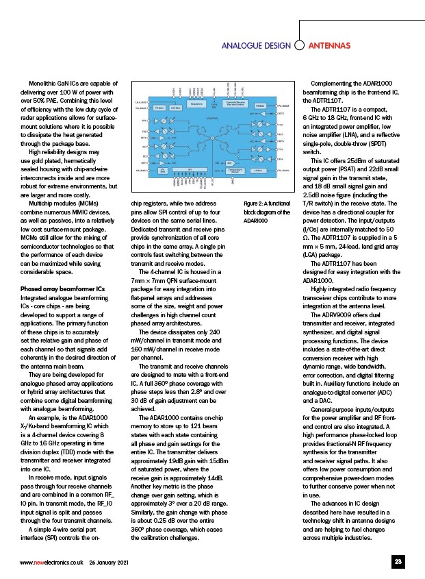
An example, is the ADAR1000
X-/Ku-band beamforming IC which
is a 4-channel device covering 8
GHz to 16 GHz operating in time
division duplex (TDD) mode with the
transmitter and receiver integrated
into one IC.
In receive mode, input signals
pass through four receive channels
and are combined in a common RF_
IO pin. In transmit mode, the RF_IO
input signal is split and passes
through the four transmit channels.
A simple 4-wire serial port
interface (SPI) controls the onchip
registers, while two address
pins allow SPI control of up to four
devices on the same serial lines.
Dedicated transmit and receive pins
provide synchronization of all core
chips in the same array. A single pin
controls fast switching between the
transmit and receive modes.
The 4-channel IC is housed in a
7mm × 7mm QFN surface-mount
package for easy integration into
flat-panel arrays and addresses
some of the size, weight and power
challenges in high channel count
phased array architectures.
The device dissipates only 240
mW/channel in transmit mode and
160 mW/channel in receive mode
per channel.
The transmit and receive channels
are designed to mate with a front-end
IC. A full 360° phase coverage with
phase steps less than 2.8° and over
30 dB of gain adjustment can be
achieved.
The ADAR1000 contains on-chip
memory to store up to 121 beam
states with each state containing
all phase and gain settings for the
entire IC. The transmitter delivers
approximately 19dB gain with 15dBm
of saturated power, where the
receive gain is approximately 14dB.
Another key metric is the phase
change over gain setting, which is
approximately 3° over a 20 dB range.
Similarly, the gain change with phase
is about 0.25 dB over the entire
360° phase coverage, which eases
the calibration challenges.
Complementing the ADAR1000
beamforming chip is the front-end IC,
the ADTR1107.
The ADTR1107 is a compact,
6 GHz to 18 GHz, front-end IC with
an integrated power amplifier, low
noise amplifier (LNA), and a reflective
single-pole, double-throw (SPDT)
switch.
This IC offers 25dBm of saturated
output power (PSAT) and 22dB small
signal gain in the transmit state,
and 18 dB small signal gain and
2.5dB noise figure (including the
T/R switch) in the receive state. The
device has a directional coupler for
power detection. The input/outputs
(I/Os) are internally matched to 50
Ω. The ADTR1107 is supplied in a 5
mm × 5 mm, 24-lead, land grid array
(LGA) package.
The ADTR1107 has been
designed for easy integration with the
ADAR1000.
Highly integrated radio frequency
transceiver chips contribute to more
integration at the antenna level.
The ADRV9009 offers dual
transmitter and receiver, integrated
synthesizer, and digital signal
processing functions. The device
includes a state-of-the-art direct
conversion receiver with high
dynamic range, wide bandwidth,
error correction, and digital filtering
built in. Auxiliary functions include an
analogue-to-digital converter (ADC)
and a DAC.
General-purpose inputs/outputs
for the power amplifier and RF frontend
control are also integrated. A
high performance phase-locked loop
provides fractional-N RF frequency
synthesis for the transmitter
and receiver signal paths. It also
offers low power consumption and
comprehensive power-down modes
to further conserve power when not
in use.
The advances in IC design
described here have resulted in a
technology shift in antenna designs
and are helping to fuel changes
across multiple industries.
Figure 2: A functional
block diagram of the
ADAR1000
www.newelectronics.co.uk 26 January 2021 23
/www.newelectronics.co.uk