ADVANCED PLATFORMS FPGA DESIGN
However, the inserted logic could
contain bugs and must be rigorously
veried.
An effective verication ow must
detect bugs as soon as possible
once they are introduced. Detecting
an RTL issue or synthesis bug during
lab testing or Gate Level Simulation
(GLS) of the place-and-route netlist
is inefcient. Moreover, the effect of
bugs introduced by implementation
tools is unpredictable. Simulation
tests are not intended to verify the
correctness of the implementation
tools, and even running all available
tests at gate-level only provides
limited condence. This approach is
indeed far from exhaustive. Finally,
debugging GLS and lab test failures is
hard and time consuming.
Formal methods are widely
recognised as a powerful and
exhaustive verication technology.
Formal design inspection and
exploration is valued for detecting
both basic and corner-case RTL
issues early and without the need for
a simulation testbench.
Automated, formal inspection of RTL
code detects issues before synthesis
starts. Unlike linting, formal tools
provide a denite answer on whether
an array may be indexed out of bounds.
In this case, the tool provides an
easy-to-debug simulation-like trace, or
counterexample, that demonstrates
how the design misbehaves.
EC tools
Formal EC tools can mathematically
prove (or disprove) that two designs
are functionally equivalent. This is
the most rigorous way to ensure that
synthesis and other implementation
steps have not introduced bugs. The
input design to the implementation
tool is typically named golden design.
The generated netlist is named
revised design.
Combinational EC largely relies on
one-to-one mapping of states between
golden (e.g., the RTL) and revised
(e.g., post-synthesis netlist) designs.
Through state mapping, the complex
problem of proving that two large
designs are functionally equivalent
can be split into a multitude of much
simpler problems: comparing the
functionality of two combinational logic
cones (see Figure 2).
The design transformations
performed by FPGA implementation
tools signicantly break one-to-one
state mapping. Formal sequential
EC algorithms can prove equivalence
of sequential logic cones, thus not
requiring state mapping. However,
while these algorithms have improved
dramatically in recent years, they do
not scale. Partial state mapping is
necessary to leverage combinational
EC wherever possible and apply
sequential algorithms only on limited
design portions (see above). In this
context, identifying corresponding
states is a crucial, challenging task.
Manual mapping is tedious and
time-consuming. Mistakes waste
engineering resources.
Formal verication signoff (see
Figure 3) enables engineers to use
advanced FPGA optimisations and
the latest synthesis technology
with condence. Formal RTL design
inspection is more powerful than
linting and nds issues early, prior
to synthesis. Formal EC proves that
the golden design functionality is
not corrupted by the implementation
step. Finally, formal fault injection and
verication supported by specialised
safety tools, can automate the
verication of safety mechanisms
in the scenarios when faults occur.
With this ow, weeks of GLS and lab
testing can be replaced with hours of
formal tool runtime.
FPGAs have long been the
hardware platform of choice in many
low-volume safety-critical applications.
Nowadays, these devices can
implement complex functions while
fullling tough performance and
power goals, competing with ASICs
also on high-volume safety-critical
applications, including automotive.
The availability of advanced EDA
tools and methodology is crucial to
support this trend. ASIC development
has used formal EC for nearly 20
years. Automated formal checks
prior to synthesis are also widely
adopted by ASIC teams. The same
technology is now available in FPGA
development, enabling a robust,
efcient implementation process.
OneSpin’s formal signoff ow of FPGA
implementation has been designed to
be orders of magnitude more rigorous
and efcient than GLS and lab tests.
The technology is mature and proven
on hundreds of industrial designs for
communications, NPPs, and other
safety-critical applications.
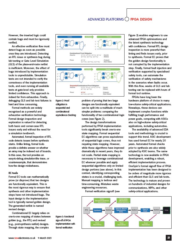
Figure 2: Proof
obligation in
sequential and
combinational
equivalence checking
Figure 3: Functional
sign-off of FPGA
implementation with
formal verification
www.newelectronics.co.uk 9 March 2021 21
/www.newelectronics.co.uk