PRODUCTS & SERVICES
Embedding MOSFETs
A new technology that uses chip embedding of power MOSFETs in PCBs
can meet increasing requirements for electrical power management systems
www.electrichybridvehicletechnology.com // July 2019 // 197
From 2021, an EU-wide
average CO2 emissions
limit of 95g/km will apply
to all newly registered
passenger cars. This will increase
demand for hybridization and
electrification. Consequently
product requirements for
electrical power
management systems with
respect to power density, energy
e iciency, reliability and system
cost reduction are increasing.
Infineon Technologies
and Schweizer Electronic
are working together to roll
out chip embedding of power
MOSFETs in PCBs. This is
a reliable way to meet such
requirements. In this process,
the power semiconductors are
embedded into a system PCB
(power and logic). It starts with
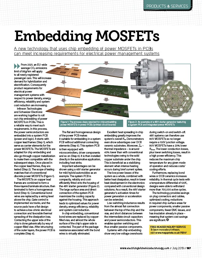
copper lead frames (Step 1), which
serve as carrier elements for the
power MOSFETs. The MOSFETs are
adapted for chip embedding and
also go through copper metallization
to make them compatible with the
subsequent steps. Once placed in
the copper lead frames, they are
tested (Step 2). The scope of testing
matches that of conventional
discrete power MOSFETs (Figure 1).
The MOSFETs on copper lead
frames are combined to form a
three-layered laminate structure, then
laminated to form a homogeneous
bond (Step 3). Conventional bond
wires are replaced by a wiring level
above the chip. Gate control is
implemented via tracks, and the
source pads have a flat design
to achieve a low-ohmic electrical
connection and favorable thermal
spreading of the dissipation loss.
Contacting the upper side of the
chip is done galvanically by way of
copper-filled vias. After structuring
of the outer layers, the power PCB is
complete (Step 4).
The flat and homogeneous design
of the power PCB makes
it suitable for embedding in a system
PCB without additional connecting
elements (Step 5). This system PCB
is then equipped with
microcontrollers, driver components
and so on (Step 6). It is then installed
directly in the automotive application,
including heat sinks.
Important advantages can be
shown using a 48V starter generator
for mild hybrid automobiles as an
example. The system PCB is
compactly, reliably and coste
iciently fitted onto the housing of
the 48V starter generator (Figure 2).
The large surface area and direct
connection of the system PCB
maximizes the cooling capacity
against the housing. This approach
leads to optimized values for power
density, energy e iciency, reliability
and system cost reduction.
In chip embedding, conventional
bond wires are replaced by copperfilled
vias, and almost the whole
surface of the chip’s upper side is
contacted. The part of the package
resistance associated with the bond
wires is virtually eliminated.
Excellent heat spreading in chip
embedding greatly improves the
system’s overall Rth. Demonstrators
even show advantages over DCB
ceramic substrates. Moreover, Zth –
thermal impedance – is around
40% lower than with conventional
technologies owing to the solid
copper substrate under the chip.
This is beneficial as a stabilizing
element when intense heating
occurs during brief current spikes.
The low power losses of the
system as a whole, combined with
better heat dissipation, result in lower
heat development in the electronics
compared with conventional design
solutions. As a result, the 48V starter
generator’s activation times for
power generation or acceleration
can be extended.
Low switching inductance results
from the almost flat connection
between the top of the chip and the
vias, and short distances between
the intermediate circuit capacitors
and power semiconductors. This
enables quicker switching and
thus smaller passive components.
Systems with chip embedding
show very low voltage overshoots
during switch-on and switch-o .
48V systems can therefore use
80V MOSFETs so no longer
require a 100V junction voltage.
80V MOSFETs have a 20% lower
RDSon. The lower conduction losses,
plus lower switching losses, result in
a high power e iciency. This
reduces the maximum chip
temperature for any given mode
of operation and reduces costs/
cooling e orts.
Furthermore, replacing bond
wires or DCB ceramics increases
reliability. In thermal cycle tests with
a temperature di erential of 120K,
designs were able to withstand
more than 700,000 active cycles.
The technology provides savings
on plug connectors and cables,
optimized cooling, reductions
in required chip surface areas for
power components, smaller passive
components, fewer EMC issues, and
has insulation already in place –
meaning that system cost savings
are significant.
FREE READER INQUIRY SERVICE
To learn more about Infi neon,
visit: www.magupdate.co.uk/PEHV
Figure 1: The process steps required for chip embedding
power MOSFETs in power PCBs (printed circuit boards)
Figure 2: An example of a 48V starter generator featuring
a system PCB and integrated power MOSFETs
/www.electrichybridvehicletechnology.com
/PEHV